Embedded Arrays
Creating hard macros for cells that are highly integrated and have advanced functionality enable development of system-on-a-chip designs, and utilization of the sea-of-gates structure in the logic means that development period subsequent to the interconnection process is roughly equivalent to that for gate array chip.
In addition, the base bulk for LSI can be deverted, in case to modify the logic block only, the lead time and cost of re-development is same as gate array.
Lineup
Design for Embedded Array Chips
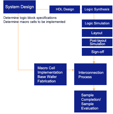
Design of embedded array chips begins from system design, determine the gate count and macro cells in the logic block .and start the base bulk fabrication. The base vulk is the wafer which the cacro cells are implemented in and the sea-of-gates logic block is laid out. On a parallel with bulk wafer fabrication, start logic and lay-out design and confirm that design through simulation. After sign-off, proceed to the interconneciotn step. The samples are shipped as same delivery schedule asr gate arrays. Since the base bulk for LSI can be deverted,Int the case of the logic modification only, it can be modified by the same development cost and time as gate arrays.
Embedded Array Lineup
S1X80000 Series
| Status | MP |
|---|---|
| Series | S1X80000 Series |
| Features |
|
| Macro Cells | RAM, ROM, Flash, LVDS, RSDS, various types of macro cells |
| Package | 48 to 256 pin QFP, PBGA, PFBGA, SQFN |
S1X60000 Series
| Status | MP |
|---|---|
| Manual | S1X60000 Series Design Guide |
| Series | S1X60000 Series |
| Features |
|
| Macro Cells | RAM, ROM, Flash, MCU, PLL, LVDS, RSDS, and various types of macro cells can be implemented |
| Package | 48-pin to 256-pin QFP, PBGA, PFBGA, QFN |
S1X50000 Series
| Status | MP |
|---|---|
| Series | S1X50000 Series |
| Features |
|
| Macro Cells | RAM, ROM, Flash, MCU, PLL, analog cells, LVDS, RSDS, and various types of macro cells can be implemented |
| Package | 48-pin to 256-pin QFP, PBGA, PFBGA, QFN, WCSP |
S1X5V000 Series
| Status | MP |
|---|---|
| Series | S1X5V000 Series |
| Features |
|
| Macro Cells | RAM, ROM, Flash, MCU, PLL, analog cells, LVDS, RSDS, and various types of macro cells can be implemented |
| Package | 48-pin to 256-pin QFP, PBGA, PFBGA, QFN, WCSP |