Silicon Foundry
Distinctive Process Technologies and Flexible Support for a Wide Range of Customization Needs Epson has been providing silicon foundry services since 1982 and has supplied products to many customers over the years. At our 6-inch and 8-inch fabs in Japan, we offer low-leakage, low-power, high-voltage, and analog/mixed-signal processes. We also have extensive experience in process transfers and provide support through production ramp-up and long-term supply.
Related Information
Process Transfer
Epson supports the transfer of customers’ semiconductor manufacturing processes to our facilities. We adapt each transferred process to our manufacturing environment and customize it to meet the customer’s specific product and application requirements.
| 6-inch Line Products | |
|---|---|
| Driver ICs, MCUs, ASICs | 3.3 V / 5 V MOS, MV MOS (~ 40 V), NV Memory, BJT |
| Ultra-Low-Power ICs | Ultra-Low-Leakage MOS |
| Power ICs | MOSFET (750 V), JFET (~ 900 V) |
| Non-Si Semiconductor Products | Si-MEMS (*1), Compound Semiconductors (*1) |
| Modules and Process Technologies for 6-inch Wafers | |
|---|---|
| 0.35 µm Generations Support | Photolithography, Process Technology, Ti Silicide |
| Al Interconnects | ~ 4 layers Al interconnects Gap Fill: SOG, HDP Planarization: CMP, Etch-Back W Plug (Etch-Back) |
| High-Current Interconnects | Thick Al Interconnects (~ 5 µm) RDL (Cu Redistribution Layer) |
| High-Precision Dopant Control (High-Energy Ion Implantation, High-Temperature Diffusion up to 1,200℃) |
|
| Special Substrate Support | SOI Wafers, Thin-to-Thick Si Wafers, Epitaxial Wafers, MEMS Substrates, Non-Si Substrates |
| MEMS Processing | Deep Si Trench, Si Lid |
| 8-inch Line Products | |
|---|---|
| Driver ICs, MCUs, Analog ICs |
1.5 V / 1.8 V / 3.3 V / 5 V MOS, MV MOS (~ 60 V), NV Memory, BJT, DMOS (Low RonA) |
| Power Devices | Diodes, IGBTs |
| Power ICs | JFET (~ 900 V), VNFET |
| Non-Si Semiconductor Products | Microlens Array, Si-MEMS (*1) |
| Semiconductor Sensors | CIS, Pulse-Wave Sensors |
| Modules and Process Technologies for 8-inch Wafers | |
|---|---|
| 0.15 µm Generation Support | Photolithography, Process Technology, Ti/Co Silicide |
| Device Isolation | LOCOS, STI, Deep Trench |
| Al Interconnects | ~ 6 lLayers Al interconnects , Thick Al Interconnects(~ 5 µm), RDL (Cu Redistribution Layer) |
| High-Precision Dopant Control (High-Energy Ion Implantation, High-Temperature Diffusion,Epitaxy) |
|
| Special Substrate Support | SOI Wafers, Thin-to-Thick Si Wafers, MEMS Substrates, Non-Si Substrates |
| MEMS Processing | Deep Trench (Deep Si Etch), Si Lid (Si Wet Etch) |
COT Process Lineup
We offer the following distinctive processes, supported by a broad range of technologies including low leakage, low power consumption, high voltage, and analog/mixed-signal integration.
We manufacture products designed by customers using the transferred design environment on Epson's process platform.
| Process Name | CMOS Mixed Signal | BiC-DMOS | ||||
|---|---|---|---|---|---|---|
| WRJ | TRY | CTX | CRC | CTC (*1) | ||
| Technology Node | 0.35 um | 0.35 um | 0.15 um | 0.35 um | 0.15 um | |
| Available Si Wafer Size | 6-inch | 6-inch | 8-inch | 8-inch | 8-inch | |
| Core Voltage | 3.3 V | 3.3 V | 1.8 V | 5V | 1.8 V | |
| I/O Voltage | 3.3 V / 5 V | 3.3 V / 5 V | 3.3 V or 5 V | 3.3 V(option) / 5 V |
5V | |
| High Voltage Option | 30 V or 40 V | 8 V | 23 V or 32 V | 8 V | - | |
| DMOS Lineup(Vds) | - | - | - | 30 V / 45 V / 60 V |
30 V / 45 V / 60 V |
|
| Available Metal Layers (Min. Layers for Logic lib.) |
3 ~ 4M (3M) |
3M (3M) |
4 ~ 5M (4M) | 3 ~ 5M (3M) | 4 ~ 5M (4M) | |
| Analog 0ption Devices (*2) | Capacitor | ✓ | ✓ | ✓ | ✓ | ✓ |
| Poly Resistor | ✓ | ✓ | ✓ | ✓ | ✓ | |
| Low-TCR Resistor | - | - | ✓ | - | - | |
| BJT | - | ✓ | ✓ | ✓ | ✓ | |
| NV Memory | - | EEPROM | OTP / EEPROM | - | EEPROM | |
| Applications | LCD Drivers, PMICs |
RTC ICs, Oscillator ICs |
MCUs, PMICs, |
Motor Drivers, LED Drivers, PMICs |
Motor Drivers | |
- *1:Under Development
- *2:Additional options not listed above may also be available. Please contact us for details.
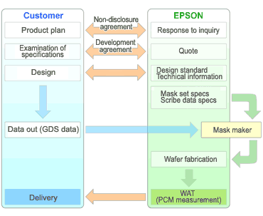
Foundry Business Flow
The standard business flow is shown below. For details, please contact our sales representative.
Contact: Microdevices Sales Department
Epson Internet Service
We provide customers with production progress and quality data for their products through our IT-based service.
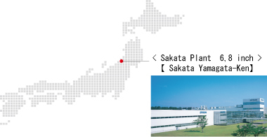
Wafer Manufacturing Plant
Shuttle Service
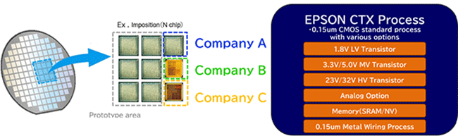
A shuttle service allows multiple customers to share masks and wafers, enabling low-cost prototyping. Epson offers this service using its 8-inch CTX process, with approximately five shuttle runs planned each year. Please contact us for details and the latest schedule.