Package Technology
This package allows you to develop lightweight and compact products friendly to the environment by integrating the super-low power CMOS LSI, that is a key device, with the high density assembly, that is a key technology. Seiko Epson has pursued the particular assembly technology by integrating super-miniaturization technology (cultivated by watch manufacturing) with low power technology, including CMOS LSI technology. Seiko Epson intends to proceed reinforcing the global and speedy technical development power and exposing information for IT and digital network society that will continue to evolve further today. Seiko Epson will timely propose the super-thin, light-weight, and high-density assembly technology as the total solution, which enhances the commercial value when you en-visage the development of products.
PFBGA (Plastic Fine-pitch Ball Grid Array) [Stacked CSP]
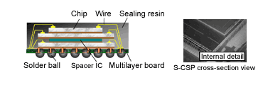
PFBGA allows you to greatly reduce the mounting area by mix and layer-stacking IC chips in one package, and to mix-load memory, microcomputer, sound source ICs and so on according to your system requirements.
Outline specifications
| Connection method | Wire Bonding Connection |
|---|---|
| Package height | 1.4mm Max. (3chips Max. + Spacer) 1.2mm Max. (Max. 2IC) |
| Ball pitch | Min. 0.5mm |
PFBGA(Plastic Fine-pitch Ball Grid Array)[Stacked CSP] Lineup
WCSP (Wafer Level Chip Size Package)
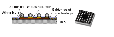
WCSP (Wafer Level Chip Size Package) is a package that satisfies lightweight, compact, and thin conditions required for high-density assembly such as a small-sized portable device. Small-to-medium-sized pin devices such as MCU, Gate Arrays, Video encoders, and USB Bus Switch ICs are targeted for applications.
- Space saving package with full real chip size
- Ball pitch: 0.65/0.5/0.4mm pitch
- Under-filling is not required because this package provides a stress reduction structure at secondary mounting.
- This package facilitates changing from a conventional interposer-type package; so, it enables you to replace bare-chip mounting (wire bonding or face-down bonding) with SMT mounting.
COF.TCM (Tape Carrier Module)
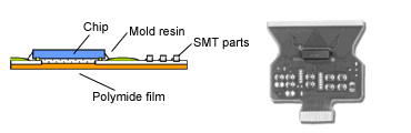
IC chips and SMT parts are mounted on a film substrate to realize not only a thin packaging but also a lightweight, compact and high-density package of high degree of freedom.
Also, gold or tin-plated lead can be bonded to gold bumps, and this inner lead bonding method has a characteristic of low impedance.
This package is applicable mainly to LCD drivers and composite modules loaded with a driver and peripheral devices and customizable with them.
- Gold or tin -plated outer lead
- Package thickness : Less than 1mm
- Ease of multi-pin use